

多功能模拟输出转接板4~20ma/0~5V
简介
8通道模拟输出4~20ma,可以通过短路帽选择电压输出0~5V,同时还包含测试代码。
简介:8通道模拟输出4~20ma,可以通过短路帽选择电压输出0~5V,同时还包含测试代码。开源协议
:GPL 3.0
(未经作者授权,禁止转载)描述
功能介绍
1.8通道模拟输出,工业标准信号(4~20ma/0~5V)
2.CAN芯片接口电路
3.24V电源控制
4.使用标准的9001-18481C00A接口,支持所有的单片机。
硬件说明:
1.模拟量输出电路
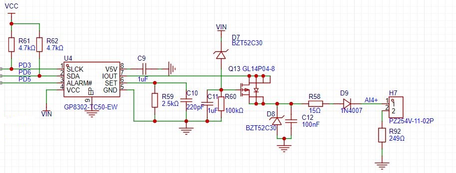
采用客益的GP8302-TC50-EW方案。
R59选择为2.5K,则全程范围内可以输出电流为0-20mA。
系统的散热通过Q13承担推荐使用SOP8封装的GL14P04-8,至少需要SOT89的封装。R58建议1206封装。
H7可以通过短路选择输出电流还是电压(不插短路帽表示输出电流)。
2.CAN芯片接口电路
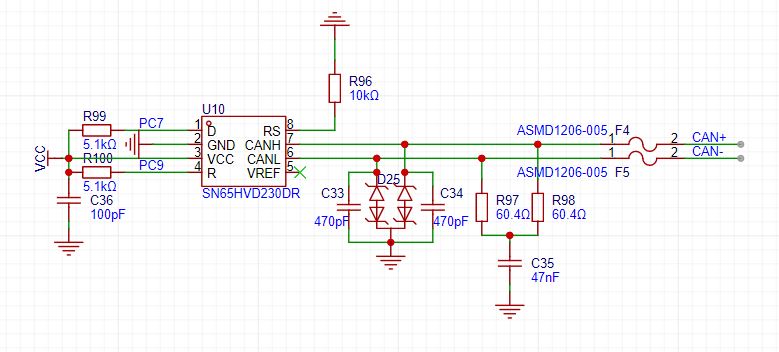
CAN芯片采用SN65HVD230DR,电源电压支持3.3V
3.24V电源控制
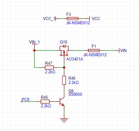
其中VCC是3.3V VIN建议电压是24V。
两路电平都采用自恢复保险丝,进行短路保护。
软件说明:
GP8302是一个I2C信号转模拟信号转换器。主板卡采用GPIO模拟IIC,本转接板可以支持不同的单片机方案。
部分代码如下:
#define POWER_PIN GET_PIN(C,8)
#define POWERCON_PIN GET_PIN(C,2)
const rt_base_t GP8302_SCLKS[] = { GET_PIN(B, 10), GET_PIN(E, 10), GET_PIN(B, 1), GET_PIN(B, 0), GET_PIN(D, 3), GET_PIN(
D, 2), GET_PIN(A, 15), GET_PIN(C, 10) };
const rt_base_t GP8302_SDAS[] = { GET_PIN(E, 15), GET_PIN(E, 9), GET_PIN(E, 8), GET_PIN(D, 7), GET_PIN(D, 6), GET_PIN(D,
1), GET_PIN(A, 8), GET_PIN(C, 11) };
const rt_base_t GP8302_ALARMS[] = { GET_PIN(E, 14), GET_PIN(E, 11), GET_PIN(E, 7), GET_PIN(B, 2), GET_PIN(D, 5),
GET_PIN(D, 4), GET_PIN(A, 11), GET_PIN(A, 12) };
/**
* The time delay function.
*
* @param microseconds.
*/
static void GP8302_udelay(rt_uint32_t us)
{
rt_uint32_t ticks;
rt_uint32_t told, tnow, tcnt = 0;
rt_uint32_t reload = SysTick->LOAD;
ticks = us * reload / (1000000 / RT_TICK_PER_SECOND);
told = SysTick->VAL;
while (1)
{
tnow = SysTick->VAL;
if (tnow != told)
{
if (tnow < told)
{
tcnt += told - tnow;
}
else
{
tcnt += reload - tnow + told;
}
told = tnow;
if (tcnt >= ticks)
{
break;
}
}
}
}
//初始化IIC
static void IIC_Init(void)
{
WRITE_REG16(CM_GPIO->PSPCR, 0x03);
GPIO_SetFunc(GPIO_PORT_A, GPIO_PIN_15, GPIO_FUNC_0);
for (uint8_t i = 0; i < (sizeof(GP8302_SCLKS) / sizeof(rt_base_t)); i++)
{
rt_pin_mode(GP8302_SCLKS[i], PIN_MODE_OUTPUT);
rt_pin_write(GP8302_SCLKS[i], PIN_HIGH);
}
for (uint8_t i = 0; i < (sizeof(GP8302_SDAS) / sizeof(rt_base_t)); i++)
{
rt_pin_mode(GP8302_SDAS[i], PIN_MODE_OUTPUT);
rt_pin_write(GP8302_SDAS[i], PIN_HIGH);
}
for (uint8_t i = 0; i < (sizeof(GP8302_ALARMS) / sizeof(rt_base_t)); i++)
{
rt_pin_mode(GP8302_ALARMS[i], PIN_MODE_INPUT);
}
rt_pin_mode(POWER_PIN, PIN_MODE_OUTPUT);
rt_pin_mode(POWERCON_PIN, PIN_MODE_INPUT);
}
//产生IIC起始信号 SCL在高电平时,SDA由高变低
static void IIC_Start(uint8_t channelNum)
{
rt_pin_mode(GP8302_SDAS[channelNum], PIN_MODE_OUTPUT);
GP8302_udelay(2);
rt_pin_write(GP8302_SDAS[channelNum], PIN_HIGH);
GP8302_udelay(2);
rt_pin_write(GP8302_SCLKS[channelNum], PIN_HIGH);
GP8302_udelay(2);
rt_pin_write(GP8302_SDAS[channelNum], PIN_LOW);
GP8302_udelay(2);
rt_pin_write(GP8302_SCLKS[channelNum], PIN_LOW);
GP8302_udelay(2);
}
//产生IIC停止信号 SCL在高电平时,SDA由低变高
static void IIC_Stop(uint8_t channelNum)
{
rt_pin_mode(GP8302_SDAS[channelNum], PIN_MODE_OUTPUT);
GP8302_udelay(2);
rt_pin_write(GP8302_SDAS[channelNum], PIN_LOW);
GP8302_udelay(2);
rt_pin_write(GP8302_SCLKS[channelNum], PIN_HIGH);
GP8302_udelay(2);
rt_pin_write(GP8302_SDAS[channelNum], PIN_HIGH);
GP8302_udelay(2);
}
//等待应答信号到来,SCL在高电平时,SDA为低电平则接受应答成功
//返回值: 1,接收应答失败
// 0,接收应答成功
static uint8_t IIC_Wait_Ack(uint8_t channelNum) //发送一个数据之后,从机必须产生应答,如果没应答,代表数据传输失败
{
uint8_t ucErrTime = 0;
rt_pin_write(GP8302_SDAS[channelNum], PIN_HIGH);
GP8302_udelay(2);
rt_pin_write(GP8302_SCLKS[channelNum], PIN_HIGH);
GP8302_udelay(2); //SCL在高电平时,SDA为低电平则接受应答成功
rt_pin_mode(GP8302_SDAS[channelNum], PIN_MODE_INPUT);
GP8302_udelay(2);
while (rt_pin_read(GP8302_SDAS[channelNum])) //如果返回1,则接受失败
{
ucErrTime++;
if (ucErrTime > 250) //如果扫描250次后仍无应答
{
IIC_Stop(channelNum); //发送停止信号
return 1;
}
GP8302_udelay(1);
}
rt_pin_write(GP8302_SCLKS[channelNum], PIN_LOW); //时钟输出0
GP8302_udelay(2);
return 0;
}
//产生ACK应答 在SCL时钟由低变高之前将SDA拉低,并保持至SCL由高变低时
static void IIC_Ack(uint8_t channelNum)
{
rt_pin_mode(GP8302_SDAS[channelNum], PIN_MODE_OUTPUT);
GP8302_udelay(2);
rt_pin_write(GP8302_SCLKS[channelNum], PIN_LOW);
GP8302_udelay(2);
rt_pin_write(GP8302_SDAS[channelNum], PIN_LOW);
GP8302_udelay(2);
rt_pin_write(GP8302_SCLKS[channelNum], PIN_HIGH);
GP8302_udelay(2);
rt_pin_write(GP8302_SCLKS[channelNum], PIN_LOW);
GP8302_udelay(2);
}
//不产生ACK应答 在SCL时钟由低变高之前将SDA拉高,并保持至SCL由高变低时
static void IIC_NAck(uint8_t channelNum)
{
rt_pin_mode(GP8302_SDAS[channelNum], PIN_MODE_OUTPUT);
GP8302_udelay(2);
rt_pin_write(GP8302_SCLKS[channelNum], PIN_LOW);
GP8302_udelay(2);
rt_pin_write(GP8302_SDAS[channelNum], PIN_HIGH);
GP8302_udelay(2);
rt_pin_write(GP8302_SCLKS[channelNum], PIN_HIGH);
GP8302_udelay(2);
rt_pin_write(GP8302_SCLKS[channelNum], PIN_LOW);
GP8302_udelay(2);
}
//IIC发送一个字节 从高位开始传输,数据传输时,SDA在SCL由低→高→低时不允许变化
//返回从机有无应答
//1,有应答
//0,无应答
static void IIC_Write_Byte(uint8_t Byte, uint8_t channelNum)
{
uint8_t i;
rt_pin_mode(GP8302_SDAS[channelNum], PIN_MODE_OUTPUT);
GP8302_udelay(2);
rt_pin_write(GP8302_SCLKS[channelNum], PIN_LOW); //拉低时钟开始数据传输
GP8302_udelay(2);
for (i = 0; i < 8; i++)
{
if (Byte & (0X80 >> i))
rt_pin_write(GP8302_SDAS[channelNum], PIN_HIGH);
else
rt_pin_write(GP8302_SDAS[channelNum], PIN_LOW);
GP8302_udelay(2);
rt_pin_write(GP8302_SCLKS[channelNum], PIN_HIGH);
GP8302_udelay(2);
rt_pin_write(GP8302_SCLKS[channelNum], PIN_LOW);
}
}
//写入数据时序:
//开始信号 -- 器件地址+写命令 -- 等待应答 -- 写入存储地址 -- 等待应答 --
//写入数据 -- 等待应答 -- 停止信号
static void IIC_Write_Data(uint8_t DataAddr, uint8_t DeviceAddr, uint16_t Data, uint8_t channelNum)
{
IIC_Start(channelNum);
//IIC_Write_Byte(DeviceAddr | 0xA0,channelNum);
IIC_Write_Byte(0xB0, channelNum);
IIC_Wait_Ack(channelNum);
//IIC_Write_Byte(DataAddr,channelNum);
IIC_Write_Byte(0x02, channelNum);
IIC_Wait_Ack(channelNum);
IIC_Write_Byte(((Data & 0x0f) << 4), channelNum);
IIC_Wait_Ack(channelNum);
IIC_Write_Byte(Data >> 4, channelNum);
IIC_Wait_Ack(channelNum);
IIC_Stop(channelNum);
GP8302_udelay(1000);
}
const uint16_t channel10mAValue[] = { 2056, 2060, 2055, 2044, 2058, 2058, 2050, 2058 };
const uint16_t channel15mAValue[] = { 3080, 3080, 3080, 3071, 3080, 3085, 3073, 3078 };
const uint16_t channel2v5Value[] = { 2068, 2068, 2068, 2062, 2068, 2068, 2062, 2068 };
const uint16_t channel3v75Value[] = { 3098, 3098, 3098, 3090, 3100, 3100, 3090, 3100 };
static void cmd(int argc, char**argv)
{
if (argc < 2)
{
rt_kprintf("Please input'cmd <channel step>'\n");
return;
}
uint8_t channelNum = argv[1][0] - 0x30;
uint8_t testStep = argv[2][0] - 0x30;
if (channelNum <= 7 && testStep <= 4)
{
if (testStep == 0)
{
IIC_Write_Data(0, 0, 0, channelNum);
}
else if (testStep == 1)
{
IIC_Write_Data(0, 0, channel10mAValue[channelNum], channelNum);
}
else if (testStep == 2)
{
IIC_Write_Data(0, 0, channel15mAValue[channelNum], channelNum);
}
else if (testStep == 3)
{
IIC_Write_Data(0, 0, channel2v5Value[channelNum], channelNum);
}
else if (testStep == 4)
{
IIC_Write_Data(0, 0, channel3v75Value[channelNum], channelNum);
}
rt_kprintf("%d %d ok\n", channelNum, testStep);
}
else
{
rt_kprintf("channel num <=7 || step <= 4\n");
}
}
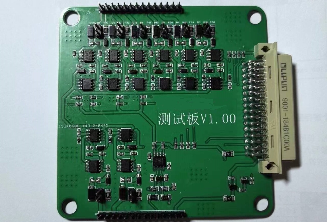
实物展示
演示视频(10ma 15ma)
设计图
BOM
 克隆工程
克隆工程知识产权声明&复刻说明
本项目为开源硬件项目,其相关的知识产权归创作者所有。创作者在本平台上传该硬件项目仅供平台用户用于学习交流及研究,不包括任何商业性使用,请勿用于商业售卖或其他盈利性的用途;如您认为本项目涉嫌侵犯了您的相关权益,请点击上方“侵权投诉”按钮,我们将按照嘉立创《侵权投诉与申诉规则》进行处理。
请在进行项目复刻时自行验证电路的可行性,并自行辨别该项目是否对您适用。您对复刻项目的任何后果负责,无论何种情况,本平台将不对您在复刻项目时,遇到的任何因开源项目电路设计问题所导致的直接、间接等损害负责。
 暂无相关工程
评论