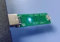
Avaota F2 双核 RISC-V 核心板
简介
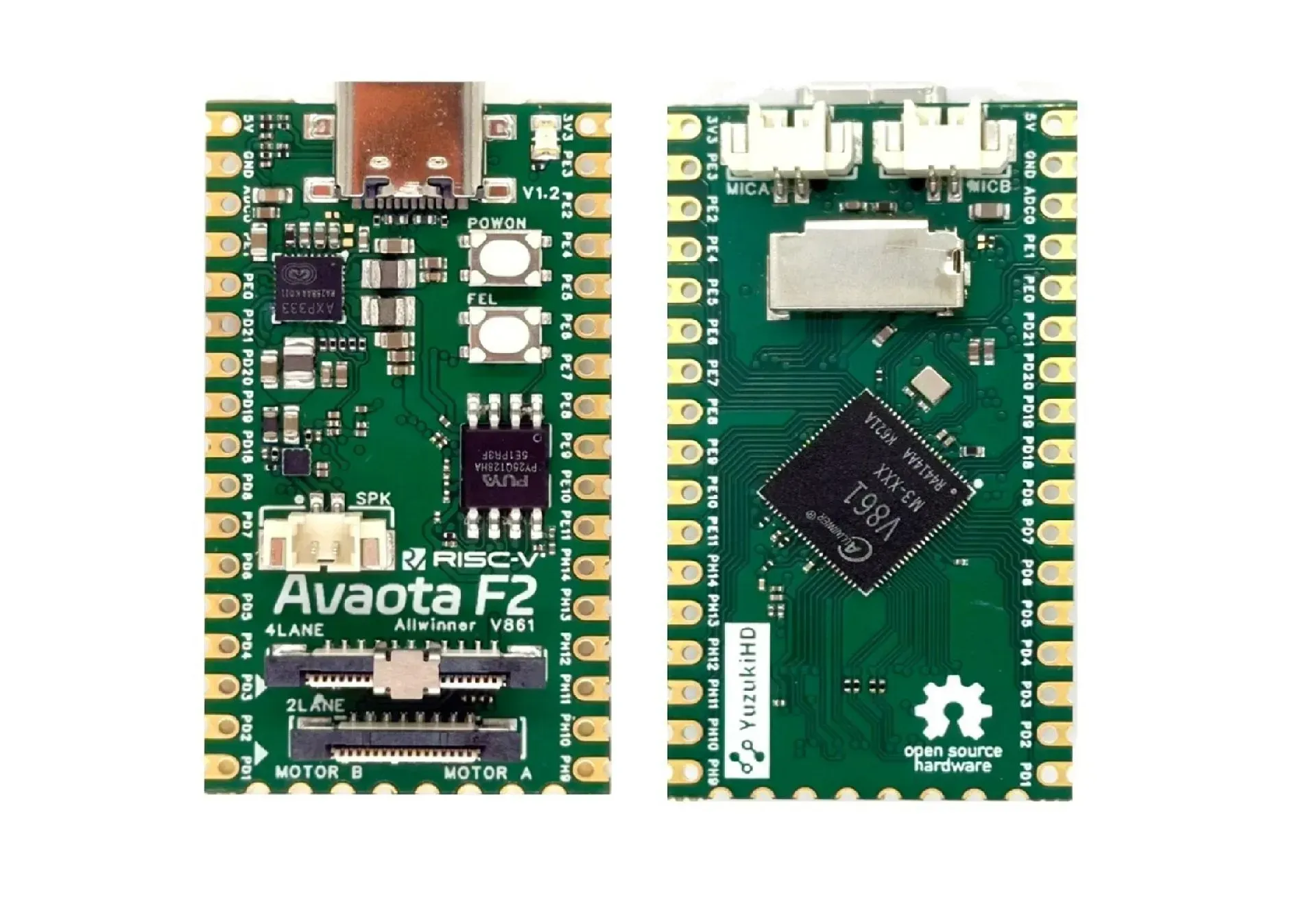
Avaota F2 是一个基于 V861 的双核 RISC-V 核心板,内置 128M 内存,Xuantie C907 核心,最大1.4GHz
简介:Avaota F2 是一个基于 V861 的双核 RISC-V 核心板,内置 128M 内存,Xuantie C907 核心,最大1.4GHz开源协议
:CC0 1.0
描述
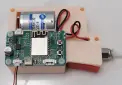
The AvaotaF2 V861 Development Kit adopts a Pico-size design, compact yet powerful. It supports a standard 2.54mm pitch header interface, making it easy to connect to a breadboard for DIY experiments. Its ultra-thin double-sided design makes it the size of a 1-yuan coin, integrating all the core features of the V861, greatly enhancing development flexibility and scalability.
License: CC0 1.0 Universal
CC0 1.0 是知识共享组织(Creative Commons)推出的公共领域奉献协议,核心是作者主动、永久、不可撤销地放弃几乎所有版权与相关权利,把作品尽可能彻底放入全世界的公共领域,供任何人免费、商用、修改、再分发,无需署名、无需付费、无需授权。
This development kit boasts several powerful features:
- Onboard MIPI CSI camera interface for high-definition image capture.
- MIC pickup function for easy audio acquisition.
- SPI NOR FLASH for sample storage space.
- TF card socket for easy data storage and expansion.
- Burn button for simplified firmware burning.
- Abundant GPIO resources that can be flexibly configured to control external hardware devices.
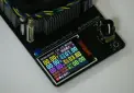
The development kit supports the latest Tina Linux 5.0 system, enabling direct development on the V861 AvaotaF2. It also supports various accessories:
- MIPI Camera GC2083 for high-quality image capture.
- MIPI Camera GC8613 for high-quality image capture.
- SPI screens: including 3.5-inch 320x480 resolution display and 1.54-inch 240x240 resolution display to meet various display needs.
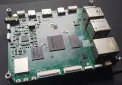
The AvaotaF2 V861 development kit integrates a wealth of features, is easy to operate, and is convenient for expansion, making it an ideal choice for embedded development and experiments.
| Item | Specification |
|---|---|
| Main Chip | Allwinner V861M2-XXX |
| PMU | Integrated power management chip AXP333 |
| DDR | Internal 128MB DDR3 |
| Memory | NOR Flash 16MB (PY25Q128) |
| Wireless | N/A |
| Camera | GC2083 1920x1080@30fps/GC8613 3840x2160@15fps |
| Microphone | Dual microphone connector |
| Button | FEL burn button / Power On button |
| LED | LED x1 |
| Debug | Supports UART serial debugging, ADB USB debugging |
| USB | Type-C USB x1, supports power, data transfer, and serial output |
| Layers | 6-layer board |
设计图
BOM
 克隆工程
克隆工程知识产权声明&复刻说明
本项目为开源硬件项目,其相关的知识产权归创作者所有。创作者在本平台上传该硬件项目仅供平台用户用于学习交流及研究,不包括任何商业性使用,请勿用于商业售卖或其他盈利性的用途;如您认为本项目涉嫌侵犯了您的相关权益,请点击上方“侵权投诉”按钮,我们将按照嘉立创《侵权投诉与申诉规则》进行处理。
请在进行项目复刻时自行验证电路的可行性,并自行辨别该项目是否对您适用。您对复刻项目的任何后果负责,无论何种情况,本平台将不对您在复刻项目时,遇到的任何因开源项目电路设计问题所导致的直接、间接等损害负责。